The top and bottom silk screen layers can now be edited to make all of the part references more legible and to add some copyright text and other message texts to these layers.
Note, when we come to do the bottom silk screen everything will look reversed as we are viewing from the top of the PCB. Let’s have a go shall we?
Close the design rules panel and open the properties panel and make sure it is pinned to the work sheet. Remember this is how `I’ do things you can always elect to work the way that feels right to you.
Open the Layers panel and check the two boxes at the bottom (I have cut out a section of the image, at the horizontal red line, to reduce it in height) labelled `Pads in Yellow’ and `PCB Filled’ then turned off all layers except the top silkscreen, and made it current, and the top layer. Then for a bit of clarity as I don’t need to see all of the tracks of the top layer (I only wanted to see the pads marked in yellow) I changed the top layer to a colour close to the PCB colour.
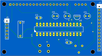
You should now have an overlay similar to this.
It doesn’t look too bad but it needs a little work.
Let’s change the size of the resistor silkscreen, right click and select SUB-PICK from the mini popup menu. The arrow should now be yellow. Click the rectangle around the resistor and in the properties you can uncheck the box `lock to courtyard’, which now allows you to change the size of this rectangle. Change the width to be 0.3” and the height to 0.1”. (If you are in cm still, select inches in the top tool bar).
Now move the part references to where you prefer them to be, I chose just under and to the left for the capacitors and U3, I moved the R1 down to be just to the right of the rectangle, I rotated U1, remember press the space bar 3 times, to be horizontal and moved it down and to the left (allow space for an IC socket).
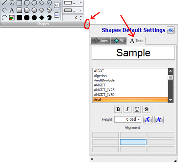
Looking at Geoff’s silkscreen he has labelled the 18pin and 4pin headers with their function. So let’s add them as well. In the ADD key tab in the tool bar, near the top of screen 2nd row, click the expand arrow at the bottom right to bring up the shapes settings and if not already selected, click the Text key tab. Here you can select your font and the font height. Set the height to 0.065” and close the settings with the `X’ at bottom left.
Now click on the A in the ADD menu which will open a text entry box and enter the text as shown in Geoff’s overlay on page 13 for the 4 pin header and then again for the 18pin one. Once entered, click on the text, to select it and in the properties panel select the Left- Justify icon, press space to rotate the text and position it under the relevant header.
Now we will add some courtesy text to give Geoff the credit he deserves.
Click the A in the ADD key tab again and type in some appropriate text. Also we need to add text for the ICSP header so add that now. And rotate it to be just to the right of the header.
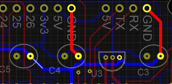
Now there is only the addition of 3 `+’ signs to add as we used a ceramic (which we fattened up for the job) capacitor in place of the tantalums. First we need to determine which side on the capacitors the `+’ should be. To do this, in the layers panel, uncheck the box `PCB Filled’, then make only the top, bottom and top silkscreen layers visible. Zoom in a bit so you have a comfortable view of the 3 capacitors and hover your mouse over one of the tracks going to any of the capacitors until you see a pop up box saying that the track is connected to the GND (or AGND as in my case) net and then single click that track. Notice how the entire GND track has now been highlighted and all other tracks are dimmed?
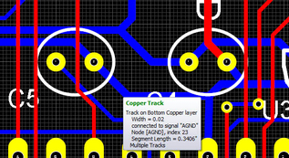
We can clearly see now that all of the GNDs are on the right hand side of each capacitor so we can make the top silkscreen `current’ (click the current check box in the layer panel) and add three lots of `+’ signs of 0.10” height and place them near the left hand pads of each capacitor (make sure that TOP SILKSCREEN is set to CURRENT).
That completes the top silkscreen.
Now the Bottom silk screen overlay.
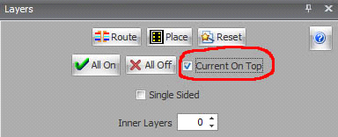
To see the silkscreen on the bottom, this is where the `Current on Top’ check box in the LAYERS panel is very useful, place a tick in there now, make the top silkscreen not visible and make the bottom layer current.
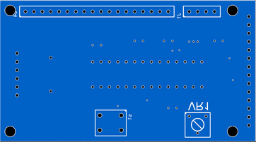
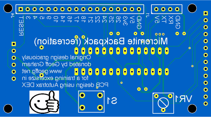
You should be able to see a view similar to this.
Make sure Current on top is checked!
As you can see there is not much here to edit but looking at my example J1 and J4 part references are rotated 180 degrees, the J4 part reference is partly over a hole, VR1 is upside down and S1 is small and rotated 90 degrees.
I will add text next to the 18pin and 4pin headers the same as we did on the top layer. You now know how to fix the position and rotation of the part references, see if you can change the font size for switch S1.
So, stop waiting for me to show you, go and DO IT!!
Did you find the slight difference with the text for the 18pin and 4pin headers? Of course you did, it was the justification had to be RIGHT justified not left justified. Don’t worry I did that too.
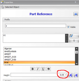
Now I haven’t spoken about how to change the font size, for S1, if you haven’t worked it out simply select the part reference (S1) and in the properties panel you will find that it was set for 0.05”, which is really quite small and probably about as small as you should ever use on PCB silk screen overlays.
Now, there is a lot of bare real estate there that we can put another credit and a bit more blurb. Hmm! Want to add an IMAGE to your design? It isn’t hard, lets add this image of a smiley with a thumbs up shall we?

To add a graphic image to the PCB silkscreen it needs to be in .BMP or .PNG format, most picture editors can convert into one or both of these formats, simple select the image icon from the ADD key tab and then select your image and, using the mouse, set the boundaries and size on the PCB. The image will drop onto the current layer.
After all those changes and edits this is what the bottom layer of my board looks like, yes everything is mirror imaged but don’t forget we are viewing from the top so it will look normal when viewed from the bottom.
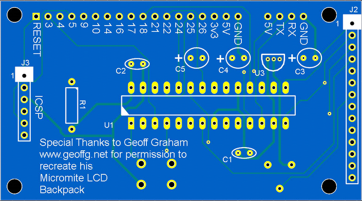
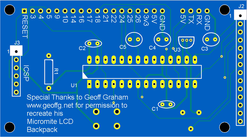
Here is the completed TOP silk screen including the added `+’ signs for the 3 tantalum capacitors.
That concludes Part 5, “Silk screens”