By now I hope that you are feeling fairly comfortable with using DEX and things are starting to feel intuitive for you.
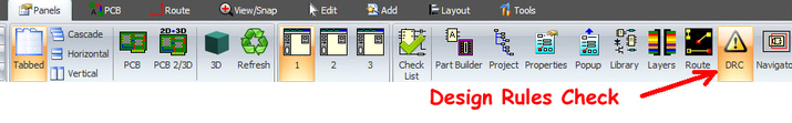
The next stage is error checking, close the properties panel, whilst having the PCB work sheet active, open the `Design Rules Check’ panel, (DRC). This can be found in the `PANELS’ key tab and is a yellow triangle icon in the middle of the tool bar.
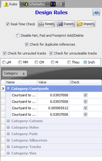
That brings up the DRC dialogue as seen here. There are 3 key tabs at the top of the DRC, the first is where you can define all of the rules that the DRC will check for. You can enter the values (e.g. clearances) or enable or disable the rule by using the check box next to each rule.
Just above the key tabs (cut from this image) there are two buttons `Check’ and `Clear’. Check will perform all of the checks and Clear will clear all errors.
Press the `Check’ button. Now you can see the errors found by clicking on the `Schematics’ and `PCB’ key tabs.
Note! Your errors may be different to mine, due to slightly different part positioning and the way Electra will handle your routing, I will go through my errors and show how I go about fixing them.
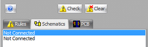
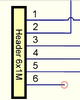
Click on the `Schematics’ key tab. This reveals I have two unconnected pins. Double clicking one of the errors opens the schematic work sheet and zooms in to show (circled in RED) the pin that has no connection. In this case that pin is unused so we can either ignore the error, or place a `not used’ marker there.
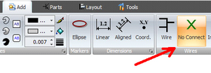
To mark that pin as not used, under the `ADD’ key tab, select `No Connect’ and place the `X’ on the pin to show it to be a deliberate `No Connect’.
The other schematic error happened to be the same but on one leg of the TrimPot. Pressing the `Check’ button now reveals `No Errors’ in the schematic.
Clicking on the PCB tab in the DRC reveals, in my case, 5 errors.
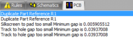
Clicking on the PCB tab in the DRC reveals, in my case, 5 errors.
Aha! The first (and 2nd) are due to a minor error in my Trimpot part. To fix this I will rename the Trimpot designator to VR1.
Auto hide the DRC panel by clicking its drawing pin/thumb tack then open the `Properties’ panel. Click on the designator `R1’ in the overlay of the Trimpot (in the PCB work sheet) and in the properties panel change this to VR1.
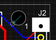
Double clicking the next error shows that the designator `U3’ (for the MCP1700), on the silk screen overlay, was located too close to a pad on the PIC’170, I simply moved this away.
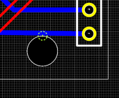
The last 2 errors proved to be two tracks that Electra decided to run too close to the drill holes as shown here.
Now we need to edit the track runs for these two tracks. In the top tool bar you will see an icon that looks like, ![]() clicking this brings up the `Layers’ panel on the right of screen.
clicking this brings up the `Layers’ panel on the right of screen.
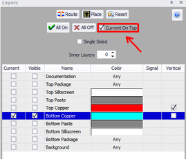
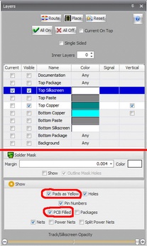
As can be seen, here you can toggle/change settings relating to viewing the layers in the PCB work sheet.
The purpose of all these are pretty self-explanatory but I will point out a small check box up near the top of the screen called `Current on Top’. This is extremely useful in the editing process when working on a board that consists of 2 or more layers (Note that Silkscreen overlays, Paste, Packages and Documentation (errors, courtyards etc) both top and bottom, are all considered LAYERS.
As we need, in this case, to work on tracks that are both on the bottom later I will select Current on Top, and have the Bottom layer as the current layer and all other layers not-visible. I have also, purely for clarity for this document, changed the colour for the bottom layer to cyan (click the colour bar, to the right of the layer name, to choose colour preference).
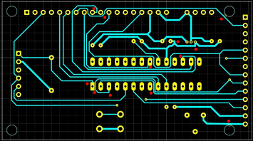
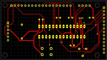
Now we can see the bottom layer ONLY. I have done a bit of photoshop and added some RED dots near the places that I am not 100% happy with. Whilst Electra does a really good job it does sometimes do some things that could have been done a bit better. Many of the red dots I have placed are because the tracks were simple a 90 degree bend instead of (my preference) 45 degree bends, a few others were where tracks are a bit close to pads and even though they passed the design rules I would prefer to move slightly.
I won’t go to great details about the way you can edit the tracks that are laid down as no amount of words can replace the lessons learned by actually doing them so instead I will offer some tips that you may chose the help with the edit process.
1.You can simply select a section of a track and move it around to a more pleasing position, all connecting track segments will move to accommodate your movements.
2.You can select a segment of a track (puts a line inside the segment) and you can right click and select ‘unroute selected segments’ then you can manual route by double clicking the net wire that will appear where the track is now broken, simple lay down a new track to suit your preference.
3.Similar to point 2, select a section of the track and right click and select `unroute track’ or `unroute net’, the difference being that `unroute track’ will remove the track that is on the side you are working on between two pads but leave any tracks on the other side untouched, whereas `unroute net’ will remove the entire net and all tracks associated with that net will be removed.. Try it, you can always `un-do’ any of your changes.
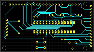
After about 5 minutes of editing the bottom layer of my board now looks like the picture on the right.
Notice that all of the right angle track bends are now replaced by 45 degree bends, some clearances are now better, the two tracks running between pins 8 and 9 of the PIC chip and the two errors (as reported by the DRC) are now fixed..
Changing the settings in the layer panel to only view the TOP layer reveals this image that I have, using photoshop, added Lime Green dots to show areas I am not happy with. In this case only 3 occurances. Two are simple 90 degree bends I want to change to 45 and the 3rd is a bit more complex, it has 2 tracks running between pins 17 and 18 of the PIC chip. Whilst there is sufficient clearance I would prefer to fix this so let’s have a try.
As you can see it is not possible to just move the track along to run between the next two pads so we will have to work with both layers to solve this one. In the layers panel tick both the TOP and BOTTOM layers as visible with TOP as the current.
Inspecting closely, I can see an easy path as shown in this image (created with photoshop).
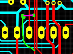
Inspecting closely, I can see an easy path as shown in this image (created with photoshop).
If I simply run the track up between pads 18 and 19 then swap layers (with a via) then I can run a track on the bottom layer to the track in question. I will also have to bend the right hand track a bit to make sufficient clearance for the 2nd via.
Ok, let’s try that, this time I will go through step by step.
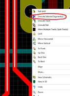
I will start by deleting the 2 segments and then reroute them. Start by clicking one of the segments, then by doing a right click to bring up a mini panel, select `Unroute Selected Segments’ then repeat with the other segment, now both of these segments will be removed and replaced by two net wires.
Starting at the bottom `broken’ segment, on the left hand track, double click the net wire to run the track up between pads 18 and 19 of the PIC and when in the clear area press the SPACE key which will place a via and you can continue your route on the bottom layer to the right, until you are in the clear again and once again press space to get back to the top layer and continue routing to the top `broken’ segment and double clicking to finish the route. Working on the right hand broken track is a lot easier as you do not have to change layers and can just route the track up (dodging the via you placed) and reconnecting with the `broken’ track segment at the top.
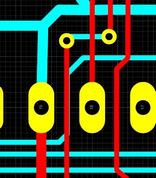
After a couple of minutes I ended up with the route looking like this image, which makes me happier as it only has one wire passing through the adjacent pads.
A re-check with the `Design Rules Checker’ now shows that there are NO errors in both the Schematic and PCB works sheets.
Some useful videos showing track editing can be found here:
In fact, it is a good idea, especially when learning, to spend a few hours reviewing the huge range of demonstration video clips that are available on the AutoTRAX DEX web site.
That concludes Part 4 – “Error checking”