Unified Design
Over the last 18 years AutoTRAX DEX PCB Designer has grown from a grassroots solution to a comprehensive PCB design software that you can rely on to produce your PCB designs quickly and have fun creating them.
It’s truly unified design gives you a 21st century application that is not antiquated like many other programs you see on the market with their clunky UI and antiquated designs which features such arcane commands as forward and reverse annotation. In DEX all your design is in one single project or part file that absolutely does not rely on any other files or library.
In AutoTRAX DEX PCB Designer there is no such thing as forward or reverse annotation. All changes you make in your schematic’s are immediately reflected in your PCB design and similarly all changes in your PCB design are immediately reflected in your schematics. Undo change in schematic and the associated changes in the PCB are automatically undone. This makes your life far easier and your design is far more reliable and error-free.
No arcane forward/reverse annotate. Absolutely not need. Changes to schematics automatically reflected in the PCB design and vice versa.
Integrated Design
AutoTRAX DEX PCB Designer is the industry’s only unified electronic design software which gives you an unmatched ability to design and build current and future generation of electronic products.
This is in sharp contrast to the previous generation of software such as Diptrace, Eagle, MultiSim, Orcad, DesignSparks and Proteus which have separate data files for schematics and PCBs – even different applications with different user interfaces.
The design of AutoTRAX DEX PCB Designer’s internal data ensures you maintain full electrical integrity with your schematic design.
Schematic Design
AutoTRAX DEX PCB Designer ensures that your design remains correct throughout with no ‘dangling wires’ or PCB design rule violations.
You can also create your own parts either in-place on your design sheets or using the integrated Part Creator. Again, design integrity is maintained throughout using DEX’s design rule checker.
PCB Design
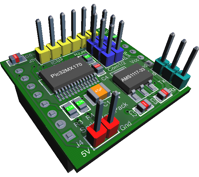
When you are satisfied with your design, you can then quickly proceed to produce your finished and populated PCB board without leaving the DEX program.
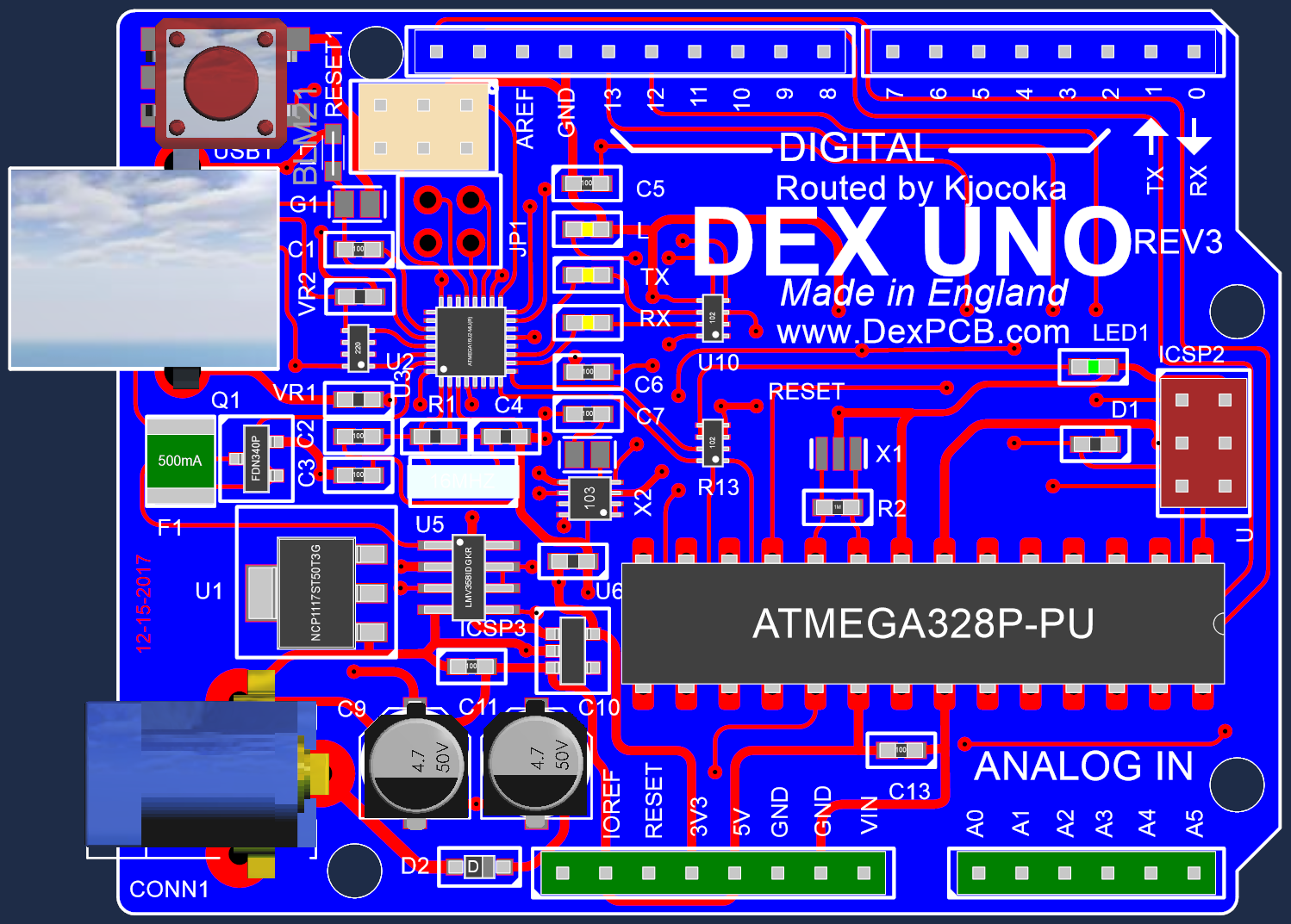
The AutoTRAX DEX PCB Designer will take your hierarchical design and place the components, with or without your assistance. Next DEX can either autoroute your board or you can use a combination of automatic and manual routing to quickly and reliably complete all electrical wiring.
Manufacturing
Now that you have your design finished and routed you can easily produce all Computer Aided Manufacturing files you will need to produce the board, drill the holes, cut its profile, order parts using the Bill of Materials, and place your parts using the pick and place files.
These files can be placed together and forwarded to your board manufacturers, electronically via email.
Unified Platform
Traditional concepts of an electronics design system haven’t changed much, at least for most EDA vendors. This can be apparent in the way they struggle to meet even the current challenges. The fragmented approach of trying to glue separate solutions together eventually breaks down as more challenges are thrown at them. It’s just unsustainable and difficult to innovate on top of inconsistent design applications that rely on constantly unmatched data exchanges. That’s not how DEX is designed.
DEX has been designed from the ground up as a powerful, single-application electronics development environment that contains all the advanced design tools you’ll need to capture and simulate hardware, design PCBs, collaborate with MCAD, manage your ECAD data and documentation, as well as manage your designs from concept to production. It’s all there in a single, unified design platform.
DEX also unifies your design data, from component models to sub-assemblies. Unlike conventional design systems based on a collection of linked tool applications, the DEX unified platform allows each design application to access and modify a single, centralized model of the design data. That’s one design project; one model of the design data; one development environment, visible to everyone. With this unified and coherent source of design data being available to all the design applications at the platform level, design synchronization and data management becomes a simple process.
Schematics
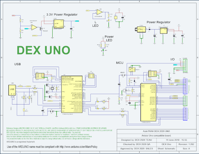

DEX’s powerful and easy to use schematic capture enables you to design your printed circuit boards quickly and reliably and be confident that the design will work. You are guided during the design process with interactive symbols, or to routing of into symbol wires and fully integrated and synchronous PCB design. Gone are the days of forward and back annotation as there is absolutely no need for such prehistoric ideas, because your design is contained in one project file: changes in a schematic of automatically reflected in your PCB layout and similarly any changes in your PCB layout are instantly reflected in your associated schematics.
Simulation
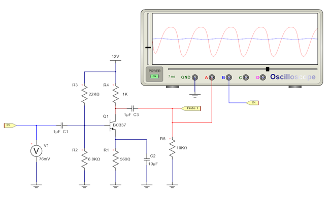
You can place real instruments such as oscilloscopes and signal generators directly onto your schematics and you will see the output and input change in real-time.
Not only is it easy to do but it is also fun.
- Real-time oscilloscope
- Full features signal generator
- Adjustable power supplies
- XSpice simulation based on Spice 3.5
Superb Graphics
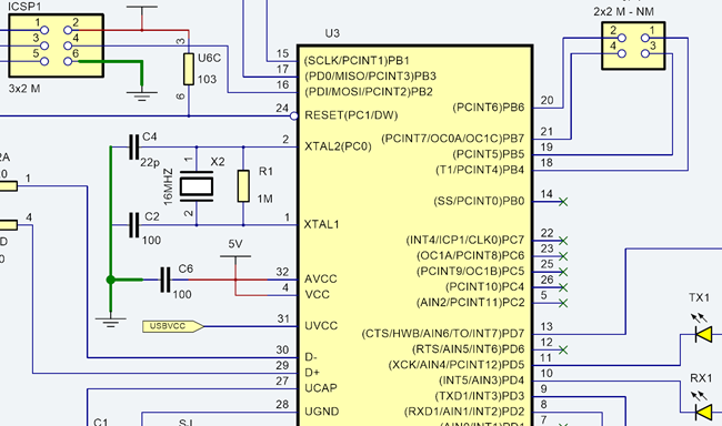

- Rich collection of graphic primitives.
- Line styles, end caps, dash patterns and colors including variable transparency.
- Solid/pattern/radial/linear multi-color fills including variable transparency.
- Full floating-point data giving you fantastic resolution.
- True-type scalable fonts.
- Excellent print quality.
Manufacturing
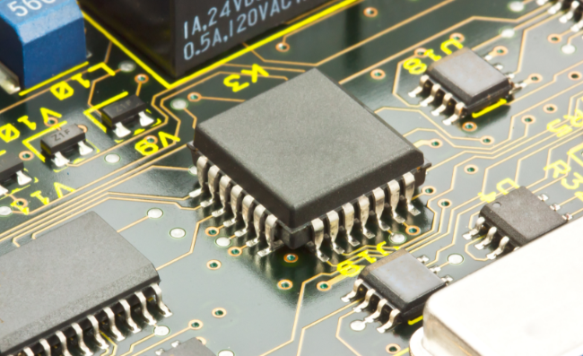

All the features you need to make your PCB including...
- Real-time DRC
- Full Gerber file output with full Gerber viewer that view your actual Gerber file; not an internal representation.
- CNC output with full inbuild CNC viewer.
- Plotting to your local printer.
Super-Easy Part Creation
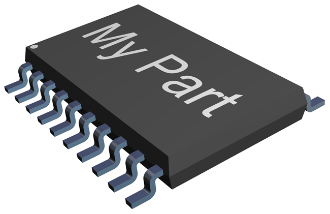

Parametric Parts
- Automatic creation of footprints from simple parameters
- 1000s of parts can be created from simple parameters, e.g. DIPs, SOICs, Quads and BGAs
- Automatic generation of 3D. No tedious searching for 3D models and importing them.
- Automatic generation of the part's schematic symbol.
- Super easy capture of pin details from data sheets.
- Use the Part Wizard to quickly create custom parts.
Active3D
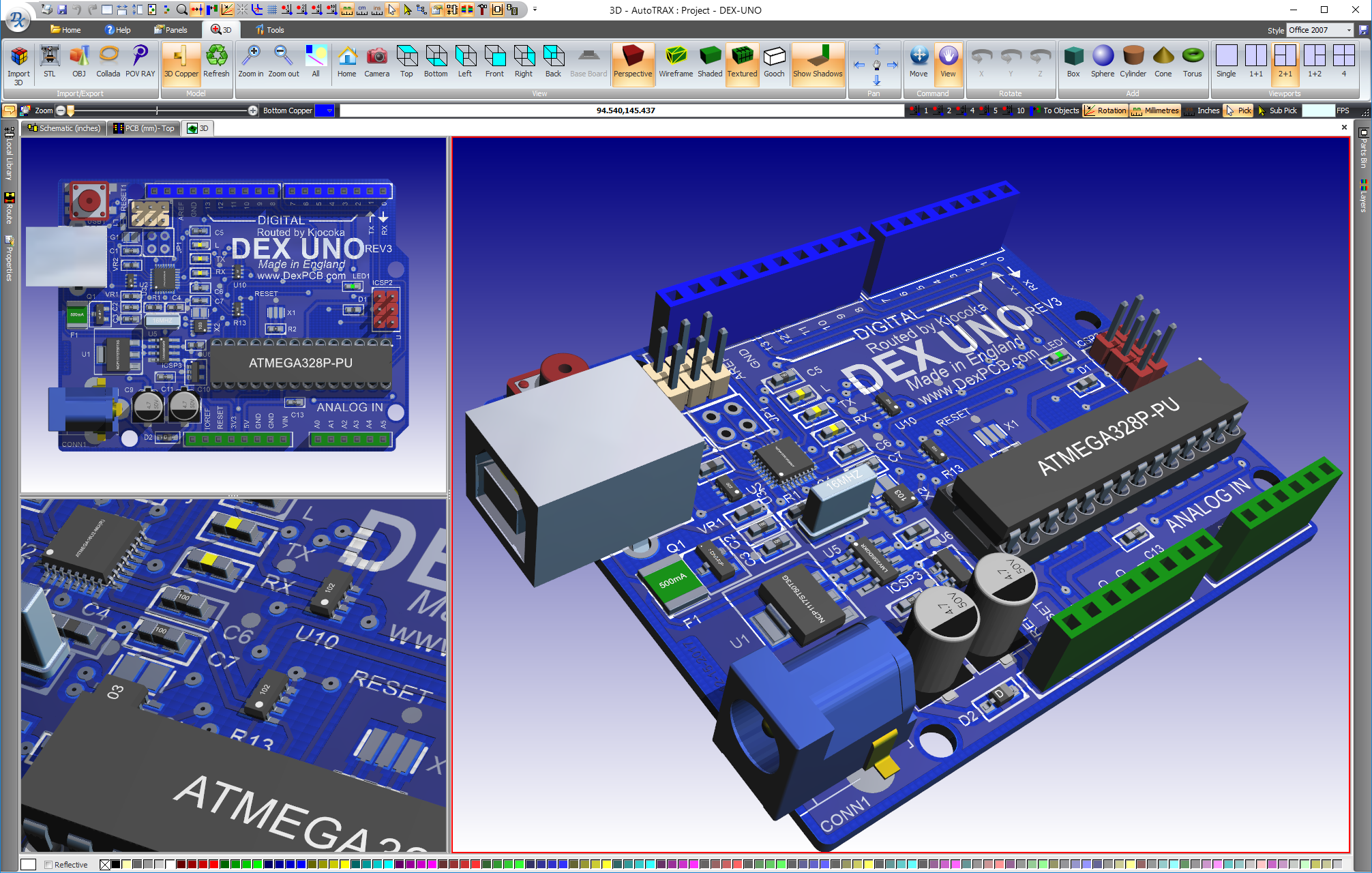
Active3D Multiple Viewports
Why put up with poor quality, unrealistic 3D views of your PCB. Instead, view your PCB in 3D with...
- Automatic generation of 3D for parametric parts. No need to import 3D models.
- real-time shadows.
- reflective surfaces.
- transparency.
- Texture mapping.
- Bump mapping.
- True 3D text.
- super-fast speed.
- and above all, super-fast, high quality imaging showing your PCB to you and the world.
Want to find out more about 3D with Active3D?
DEX DEX with Active3D
High Performance PCB Design Made Simple
Empowering you to create electronics-based products for a smarter, safer, and more connected world.
 Overview
 Unified Design
 Schematics
 Graphics
 Parts
Parts Simulation
 PCB Designer
 PCB 2D
 3D
3D Manufacturing
