OK! Let’s get down to business. Load up DEX, you will notice that if you have already had a play your last saved design will automatically load for you. We will want to start afresh so up near the top left hand side of the screen you will see an icon that looks like a blank page with a wand on it, this is the create new project icon. Click here and a new project will open for you.
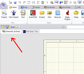
The screen should be now displaying a blank graph sheet with two tabs showing Schematic and PCB, you can select whether the active screen is schematic (as we want now) or PCB area, try it… But go back to Schematic to start the next step.
LOAD PARTS on Schematic
Now we need to open our library, along the very top row you will see a whole bunch of small icons, the library is the one that looks like a few components. This should open the library panel on the left hand side of the design sheet.
![]()
NOTE!! Clicking the icon again will close the library panel (all of those icons work as on/off toggles) Also you will see a little drawing pin/Thumb tack on the top right of the panel. This will pin the panel or allow it to collapse to a tab on the left hand side. For simplicity we will keep the panels pinned, and opened or closed, as we need them, it can be a bit confusing initially with all these tabbed panels.
Drag your parts onto the schematic
In the `docked’ library panel on the left you should be able to see a list of directories containing parts. You should be able to navigate to your library and find the parts we copied into there. Click and drag the following parts onto the schematic work sheet. You are free to arrange the schematic as your prefer it is all free and flowing there is no set order for placing parts on the schematic, in fact the layout I show may not be optimal.
PIC32MX170,
TrimPot,
Switch Tactile (4pin),
4pin MALE header,
18pin MALE header,
6pin R/A MALE header,
14pin FEMALE header
MCP1700 Voltage Regulator.
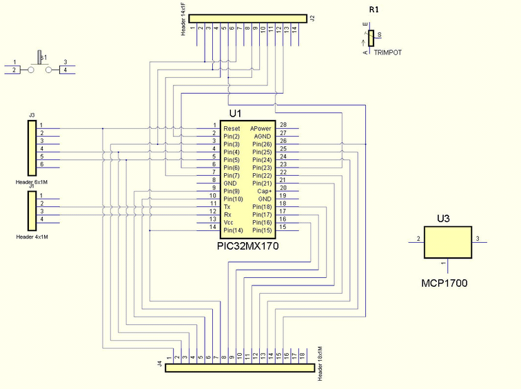
I have initially placed my parts as shown below, these can be moved and rotated to suit your preferences, the text in RED is added for clarity but will NOT appear in your schematic.
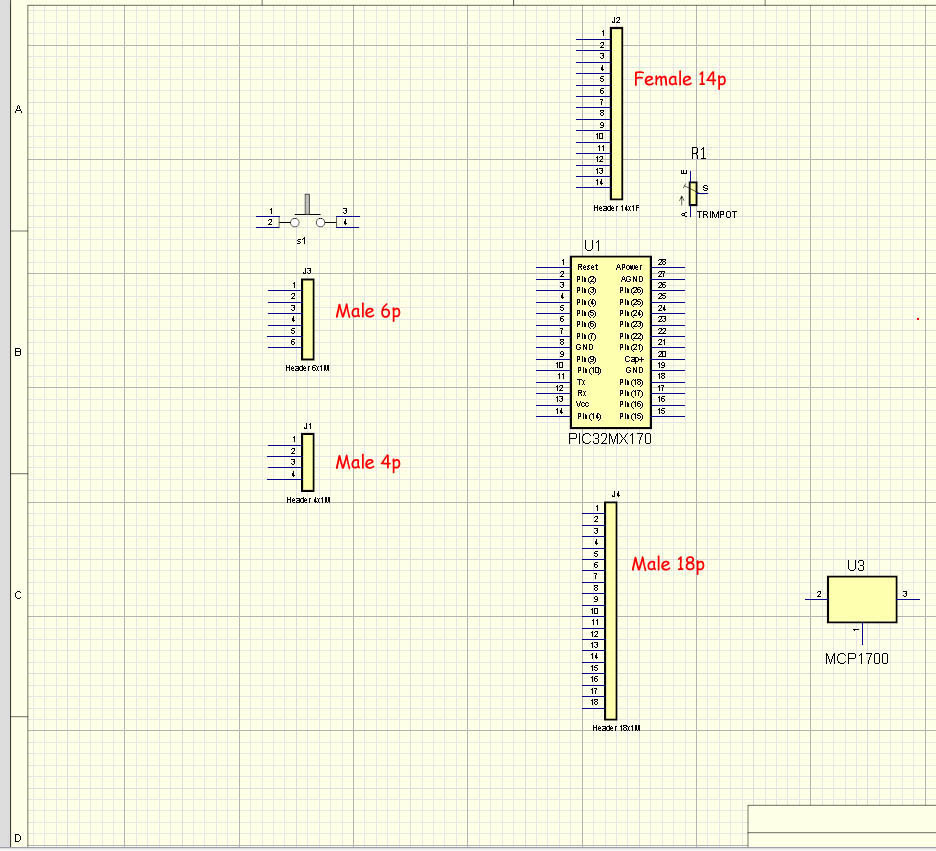
You will note that every one of the headers happen to have defaulted to an alignment that is not ideal.
To position the headers to a more ideal alignment do the following in order.
First a bit of a tip! If your arrow pointer is WHITE then you are in `PICK’ mode this will select the entire part for movement/rotation, if you right click you can see in the mini-menu `SUB Pick’ this turns the arrow YELLOW, in this mode you can select a small component of the part, such as the pin, to move it into a more ideal position on the schematic symbol. Try it and have a play but put it back the way it was when you are finished. These changes will make no impact on the physical footprint of the part on the PCB. Right click to select `PICK’ again when done.
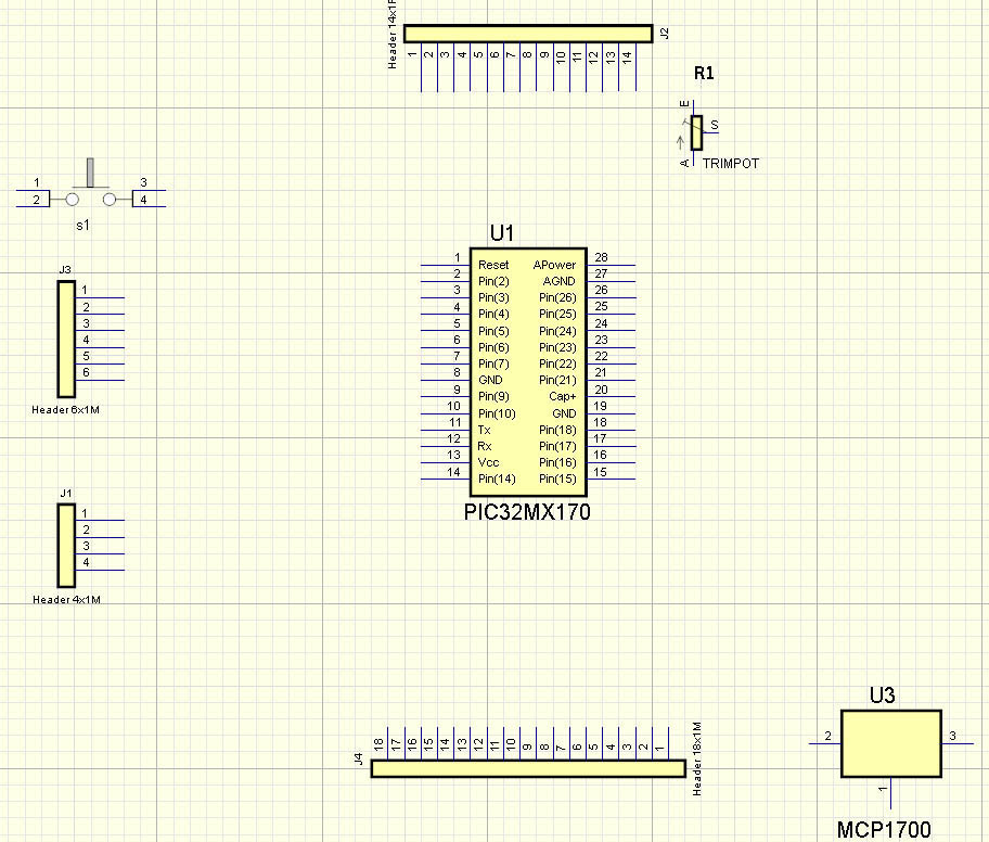
Click on the MALE 18pin header, then press space once, that part will rotate and be in a better position to connect to the PIC chip. The FEMALE 14 pin can be selected and hit the space 3 times to rotate it to point towards the PIC chip.
With the MALE 4pin and MALE 6pin R/A I think it might be better if we `FLIP’ the part rather than rotate as the pins would line up better to the PIC chip. To do this select the part and RIGHT-CLICK and select `Mirror-Horizontal’ this will change the pins from the left hand side to the right hand side of the part but keep their order. You should then end up with something like this.
Wiring the parts together.
We are now ready to wire up our design, I refer you to Geoff’s original schematic attached in APPENDIX A for reference. You will notice that Geoff has not put pin numbers on his header pins (except header CON4), that is fine but we will assume that pin 1 is at the TOP (in Geoff’s schematic) for each header. To this end we should `FLIP’ the MALE 18pin header to simplify wiring. (The picture above shows it BEFORE we flipped).
I refer you to the following video clip (there are many good clips on kov.com/Videos to peruse)
Here we need to connect our wires up (and add a few `glue’ parts such as resistors and capacitors).
Go through and connect the wires as per the schematic in APPENDIX A by clicking a pin on one part and then moving to the relevant pin where it needs to connect to, and the wire will automatically join up. Don’t route any power or Gnd signals just yet, we will do them differently after the other tracks are run.
TIP! If you lift your finger off the mouse your wire will lock in place and you can route it in another direction and keep the previous part of the run fixed in place. Of course you can move them later if needed.
Hopefully you found that fairly easy to route and you have ended up with something that looks like the following.
NOTE! I have turned off the grid, for clarity, for the screen capture, this is done by the ![]() icon on the top tool bar. Like all of those top icons, clicking this icon turns it on and off alternatively. You will see all of the power connections still need to be made.
icon on the top tool bar. Like all of those top icons, clicking this icon turns it on and off alternatively. You will see all of the power connections still need to be made.
Adding Parametric Parts
DEX has many built in parts that make building your PCB much more convenient, these include capacitors, resistors, power symbols, transistors etc.
We will now add the power symbols to our schematic. You can close the library tab by pressing the X in the top right corner of the LIBRARY Panel or alternately clicking the ![]() symbol in the top tool bar.
symbol in the top tool bar.
In Geoff’s original schematic all of the Power signals are physically connected, in my PCB I am going to use Power Ports, found in the Parts TAB. I also like to use the ANALOG GND port as I prefer that symbol instead of the digital one but that is all user preference.
We can now open the PARTS TAB, located on the tool bar, 2nd row. That brings up the parametric/generic parts list.
By using power ports is simplifies the look of the schematic so that it is not cluttered by all the power and GND wires crisscrossing the page. All pins connected to a power port will be deemed to connect to every other pin that is connected to the same type of power port.
I will be using the following power ports for my schematic.
![]() For 5V pads (Note it will place as BLACK, the RED colour is so you can distinguish it from the -5V port.
For 5V pads (Note it will place as BLACK, the RED colour is so you can distinguish it from the -5V port.
![]() For Vcc (3v3) pads
For Vcc (3v3) pads
![]() For GND Pads
For GND Pads
Now select the 5V port from the parts tab and place them near where they are needed to be connected to pins on the various parts and wire them to the appropriate pins.
In this design 5V goes to the following places:
Pin 1 of the 4pin male header
•Pin 17 of the 18pin male header
•Pin 14 of the 14pin Female header (I really think this should be Vcc but we will stick to the original design)
•Pin 2 of the MCP1700
•One side of the TrimPot
•Now locate the places where Vcc and GND need to have power ports and position them in suitable locations, you may need to move parts around to squeeze them in, and wire them up.
You should now have something that looks like this.
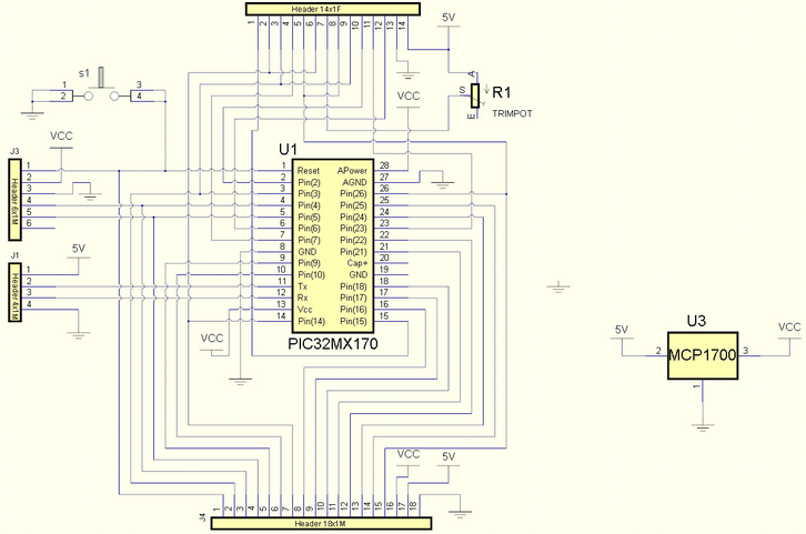
Our Schematic is now almost complete, we only need to add a few capacitors and a resistor to our design.
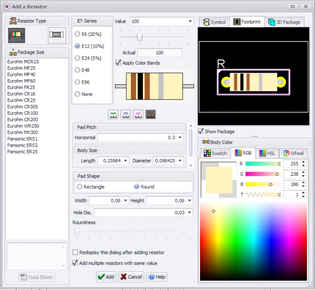
First we will add a resistor, select the designator you prefer for your resistor from the parts tab and a menu box will open that looks like this one. Here you can set all of the properties for your resistor, such as:
•Axial or SMD chip in the top Left of the panel.
•The Value in Ohms in the top centre of the panel.
•The Horizontal pitch, pad shape, size and hole diameter and a few other fairly obvious settings.
We will choose, AXIAL, 0.4” pitch, round pads 0.06dia with a 0.03” hole.
When the settings are complete select ADD and place in on your schematic in a suitable location near PIC pin 1 and the reset switch/
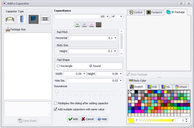
Now we need to add the Capacitors. As per the resistors above, select the designator (non-polarised) you prefer for your capacitor from the parts tab and a menu box will open that looks like this one. Here you can set all of the properties for your capacitor, such as:
•Through hole (or SMD) in the top Left of the panel.
•The Value in the top centre of the panel.
•The Horizontal pitch, pad shape, size and hole diameter and a few other fairly obvious settings.
We will chose, through hole, block capacitor, 0.1” pitch, 0.1” height, round pads 0.06dia with a 0.03” hole. You can also change the colour of the part from the colour palette in the bottom right hand corner.
As we are going to add 2 capacitors of 100nf value check the box for `add multiples’ and then drop both of them on your schematic, I suggest placing them somewhere on the right hand side of the MCP1700 voltage regulator.
Press ESC after you have placed the second capacitor on the schematic.
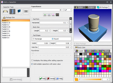
We can now add the 2 x 10uf capacitors and 1 x 47uf. So select the designator you prefer for your capacitor from the parts tab and a menu box, this time a polarised symbol. As there is no TANTALUM image I chose an electro image, change the settings again for the value, size, pad shape, pad size, hole dia. (I chose 0.1” pitch, 0.2” length, 0.3” high and .06” round pads with .03” dia. holes). Check the box for `add multiples’ and then drop them on your schematic And place 1 capacitor on the left of the MCP1700 and another on the right of the MCP1700 then a 3rd to the right of the PIC’170 (this will be for the 47uF capacitor). Lastly we just need to change the value for the last capacitor we placed to be 47uf, do this by selecting the capacitor, then clicking the `properties’ icon ![]() , from the top tool bar, which opens the properties panel, and changing the value to 47uf (from 10uf). We could have gone through the entire process of selecting another capacitor and changing its value and all the other settings but I feel this was much easier.
, from the top tool bar, which opens the properties panel, and changing the value to 47uf (from 10uf). We could have gone through the entire process of selecting another capacitor and changing its value and all the other settings but I feel this was much easier.
Now all that is needed is to connect up the wires to the resistor and the 5 capacitors we placed (beware of polarity of the 3 polarised ones) and you should have a schematic that looks something like this.
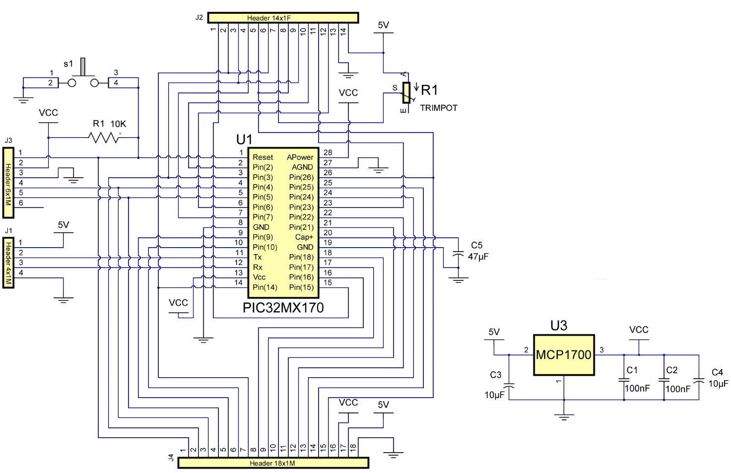
Yours may look a bit different than mine, it all depends on how you ran your wires and your personal preferences in layout styles. As I said at the start of this document, this is how `I’ do my boards. I am 100% certain that I am not using DEX to its fullest extent and even this morning I saw someone post on the DEX forum a PIC32MX170 part where he imported an image into the schematic part and it looked magnificent. I never thought to do that. That is something I can add to a `Tips & Shortcuts’ document.
Now you may ask, Why did I choose electrolytics instead of the Tantalums? Well, it really doesn’t matter what I chose for the 3D representation as it can be changed later on at the PCB creation stage of this Document. At this point in time there doesn’t appear to be a tantalum capacitor in the parts list so I will ask the author if he can add one. And in the interests of visual perfection I intend to show later how we can import a 3D model for a part that we do not have in our 3D repertoire. What is important is the physical pad sizes and spacing and hole diameters and even these can be changed later in the project.
That concludes Part 1, “Schematic”