Click on the PCB key tab and you should see a PCB layout with all of your parts spread around the outside.
You probably won’t see all of the parts in the display area, if you don’t you can zoom in and out with the mouse wheel and navigate around with the arrow keys (you need to click in the screen area first before the arrows work).
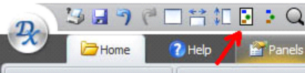
TIP! There is an icon in the top tool bar that will show all objects in the screen view port. Also if you hover over Any icon you will see A short description.
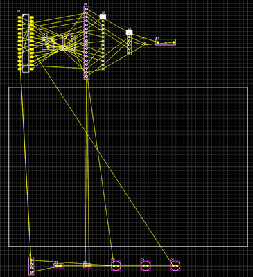
The yellow lines show all of the NETs that have been
Auto generated from your schematic, the white box signifies your PCB. Along the top tool bar there are a few icons that select various settings/modes of operation.
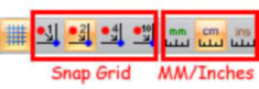
I have selected 2 snaps per grid (0.05”, this is always an imperial measurement), and elected to use cm. Have a play with these settings, there are several more that serve other useful purposes that I won’t go into in this document.
Now if we select the PROPERTIES panel and pin it in place (remember the drawing pin/thumb tack), we can select the PCB outline and size it to suit our application.
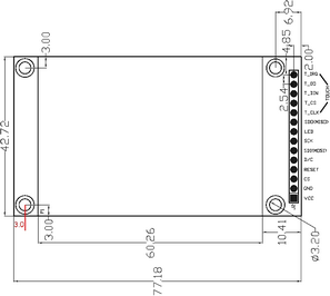
Using this diagram we can see that the PCB should be 7.718cm x 4.272cm. Note there was 1 missing dimension, marked in RED, I have assumed this to be 3mm, and for this this exercise will be close enough.
Now you should be able to see in the properties panel various properties pertaining to the PCB itself.
We will set the origin![]() to the bottom left corner (not needed generally but for positioning the mounting holes it makes it much easier). You will see a check box for add mounting holes but we will add them manually.
to the bottom left corner (not needed generally but for positioning the mounting holes it makes it much easier). You will see a check box for add mounting holes but we will add them manually.
As you may notice, here you can set the shape and colour of the PCB and the colour of the solder mask.
Firstly we will define the width and height of the PCB by entering the values into the relevant sections of the property panel, (w=7.718, h=4.272). Then if we click the button up near the top of the property panel we can set the origin to the lower left corner. If you can’t see that button then you probably have the `Selected object’ pulldown minimized. Click the chevron on the right to expand this section.
![]()
TIP! You can enter values 3 different ways:
1. By highlighting the complete value and entering from the keyboard.
2. By clicking the `pull down’ arrow and using the mini `pop-up’ keypad.
3. By clicking to the right of any of the numbers and scrolling up & down using the scroll wheel.
You should now see a PCB outline that looks the same shape as the PCB we are going to design and that the lower left corner is sitting at the 0,0 (origin) position on the rulers.
TIP! You can toggle many view options on & off by clicking in the View/Snap key tab.
For this exercise, I will set the following view options:
Rulers ON
Courtyards OFF
Placement OFF
Nets OFF
You can elect to set any on or off as pleases you, I have selected the above to minimise cluttering the work area.
We will now manually add 4 mounting holes and then position them as per the template on page 10.
In the ADD tool bar select `Drill Hole’ in the CUTOUT section, this is where you can define areas of your PCB to have drill/mounting holes and cutouts etc.
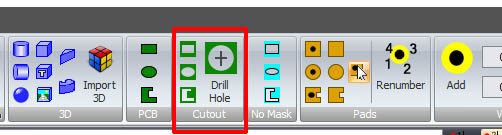
Now add the 4 drill holes of 0.32cm Dia. to the PCB (should have turned a solid BLUE), placing them roughly where the holes should be, no need to be exact we will reposition them in the next step.
As we previously set the bottom left corner to be at 0,0 we can calculate the correct location for each hole as (starting at the hole on the bottom left as 1 and going to each in a clockwise direction).
Hole 1 is located at 0.300, 0.300
Hole 2 is located at 0.300, 3.972
Hole 3 is located at 7.026, 3.972
Hole 4 is located at 7.026, 0.300
Select each hole in turn and using the PROPERTIES panel, enter the X and Y coordinates for each hole as per the list above.
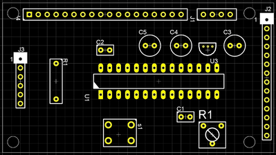
Your PCB and hole locations should now look like the image of the PCB on page 10. If not then you have missed a step or entered some incorrect coordinates.
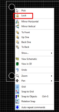
This has set the physical boundaries of our PCB and mounting holes. We now want to LOCK these in place to prevent accidental movement whilst we are manipulating the other components.
To accomplish this in DEX, select each item (each hole and the PCB border) in turn and then right click to bring up this menu and select LOCK.
Now these items cannot be accidentally moved and we can carry on with moving our parts on the PCB.
Loading the Parts
This stage of the PCB design just cannot be easier (unless you select `Auto Layout’ in the LAYOUT key tab), have a play, you can’t hurt anything. When you are finished have all the parts off the board ready to start loading them onto the PCB.
TIP! DEX automatically backs up EVERY thing you do into a backup directory, located in the directory your project is saved to. In our case the directory will be called `DEMO.BACKUP’. If you really get yourself in a mess you can always load one of your backups from a time where you were happy with your design. Also in the top tool bar there are the ubiquitous `Un-Do’ and `Re-Do’ arrows, as well as Ctrl-Z for Un-Do.
There is only one part that needs care when it is placed onto the PCB and that is the 14pin header. This is because our board is designed to connect to a commercial display module that is fixed in its position to the PCB boundary and the mounting holes. We will need to position and correctly orientate this header, and LOCK it in place, before we start loading the other components onto the PCB. As the diagram on page 10 shows the top pad to be 0.485cm from the top of the PCB and 0.200cm from the right hand side, by simple calculations we know the centre will need to be located at 7.518, 2.136. DEX defaults to have the placement point at the centre, this can be changed to suit user preference.
Let’s grab the 14pin header and drag it onto the PCB and rotated so that Pin 1 is facing UP (remember, earlier, from in the schematic, we can rotate parts by selecting them then pressing the space bar until they are rotated in the direction we want). Once the Female 14pin header is placed on the PCB in the correct orientation (pin 1 UP) we
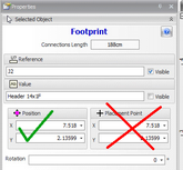
can then enter the location in the PROPERTIES panel. Then LOCK it in place!
WARNING!!
Enter the coordinates in the POSITION section NOT the PLACEMENT POINT, as shown. (If you change the placement point settings you will move the placement point NOT the part).
=======> Mea Culpa !! <=======
It transpires that the assumption I made on page 4 regarding pin 1 facing UP is actually incorrect, however we will live with that mistake as we are committed with the schematic as it is and electrically it will be OK. This is a learning exercise after all.
Now Place all of the other parts in a location close to the original board design that Geoff designed as shown below, I have marked the Pin 1 for the 4pin and 18pin male headers. Exact position is not necessary, as there is no need to mate with the LCD display.
NOTE! This image is for the 2.8” TFT backpack, our design recreation is for the 2.4” unit.
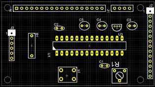
You should now have everything laid out and looking something like the picture below:
Having a close look reveals one obvious inconsistency with the parts, the MCP1700 TO-92 part has some very small pads. This is a perfect time to show how you can edit these with SUB-PICK. Right click anywhere in the work area and select Sub Pick, the cursor should turn yellow, then with the properties panel open click on each of the 3 pads and change them to 0.09cm width and height and 0.05cm dia. hole.
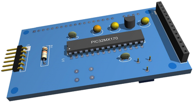
Let’s have a sneak peek at the 3D at this stage (I know you have been champing at the bit for this). If you don’t already have a 3D work sheet available right click in the PCB work sheet and select `View in 3D’ (zoom in and out with the mouse wheel and navigate with the arrow keys) and you would then see something like this image.
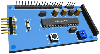
Things we observe here are the 4pin and 18pin Male headers are facing up, they should be on the other side on the PCB and as I have decided to use a horizontal TrimPot it will not be possible to adjust with the LCD module in place so we will flip this to the other side as well, also we will deviate from Geoff’s design a bit here now and flip the mini tactile switch to the other side as well.
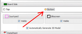
To do that, have the PROPERTIES panel selected and whilst in the PCB work sheet, click on each of those parts and toggle them to the BOTTOM layer. A quick check of the 3D view will show these are now swapped onto the bottom side of the PCB. We are now almost ready to route the board.
Just before we route the board, let’s change the 2 x BLOCK capacitors for Ceramic Disk and the 3 x Electrolytic capacitors for something that looks closer to a tantalum.
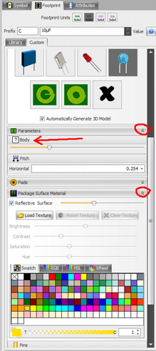
In the PCB work sheet, close the PROPERTIES panel and open the PART BUILDER panel. Now click on one of the 100nf capacitors and click on the shape that looks like a blue ceramic capacitor.
You should see the outline of that capacitor change to an oval shape and the pads change to square, scroll down in the PART BUILDER panel and change the pads to round. Now let’s change the colour, scroll down a bit more and you will see a minimized chevron with the name `Package Surface Material’ open this and change the colour using one of the colour selection options, (I chose `Dark Khaki’). Repeat this for the other 100nf capacitor.
With the 2 x 10uf a 47uf electrolytic I am going to do the same and change them to a disc ceramic BUT I will `fatten them up’. How? Let’s do it! Click a 10uf and change to a disc ceramic and set pad shape and colour (I chose Gold) as before but immediately under the PARAMETERS chevron pull down you will see a slider that says `? Body’, slide this until you are happy with the fatness (I chose a point about 1/3 the way across). Repeat this for the other 10uf and the 47uf capacitor (I chose Orange for that one).
Have a look at the 3D view now, look better? Alright I know the tantalum doesn’t look perfect and I have asked Iliya to provide one in the parametric parts. In any case in the 3D section later in this document I will go into how you can import a 3D object to your design.
Your PCB view and 3D view should look pretty close to these examples here. Note the fatter `tantalum’ capacitors.
That concludes Part 2,“PCB”.